Researchers Develop New Atomic Force Microscopy Technique
Scientific breakthroughs help us to understand the world around us, and how materials interact on a variety of levels. But, in order to discover these new concepts, or refine our understanding, we constantly need new technology to visualise and capture accurate data.
A research team from the University of Tsukuba in Japan is once again at the forefront of scientific advancements with its development of a new time-resolved atomic force microscopy technique (AFM).
The team was previously responsible for the development of a time-resolved scanning tunnelling microscopy (STM) technique, which allowed scientists to observe materials with nano-spatial resolution and femtosecond temporal resolution. However, this technique relies on materials allowing an electrical current to flow between the probe and the sample being observed – which limits its use to electrically conductive materials.
To combat this, and allow for a wider range of samples to be examined, the research team developed a time-resolved AFM method by combining traditional atomic force microscopy with unique ultrashort laser pulse technology. By removing the reliance on electrical currents, this method allows scientists to work with more materials, including insulators.
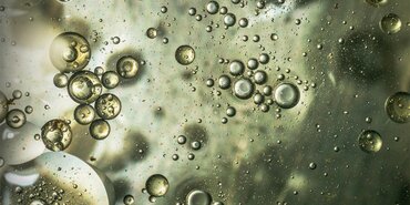
Using its method, the team was able to measure the ‘dynamics of surface recombination and diffusion of photoexcited carriers in bulk WSe2’. Tungsten diselenide is a semiconductor, and is challenging to use in conventional time-resolved STM because of ‘the effect of the tunnelling current’.
There are plenty of valuable future applications for this new microscopy technique. For example, understanding the behaviour of photoexcited carriers can help scientists to develop or improve solar cells and photodetectors. It may also assist with improving semiconductor devices like those which ‘underpin ultra high-speed communications and artificial intelligence (AI)’.
Additionally, by broadening the technology on hand to observe phenomena, new branches of different scientific disciplines could be generated, and more discoveries and refinements to existing knowledge could come in the future.
Advanced microscopy at The Lab
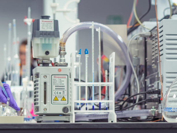
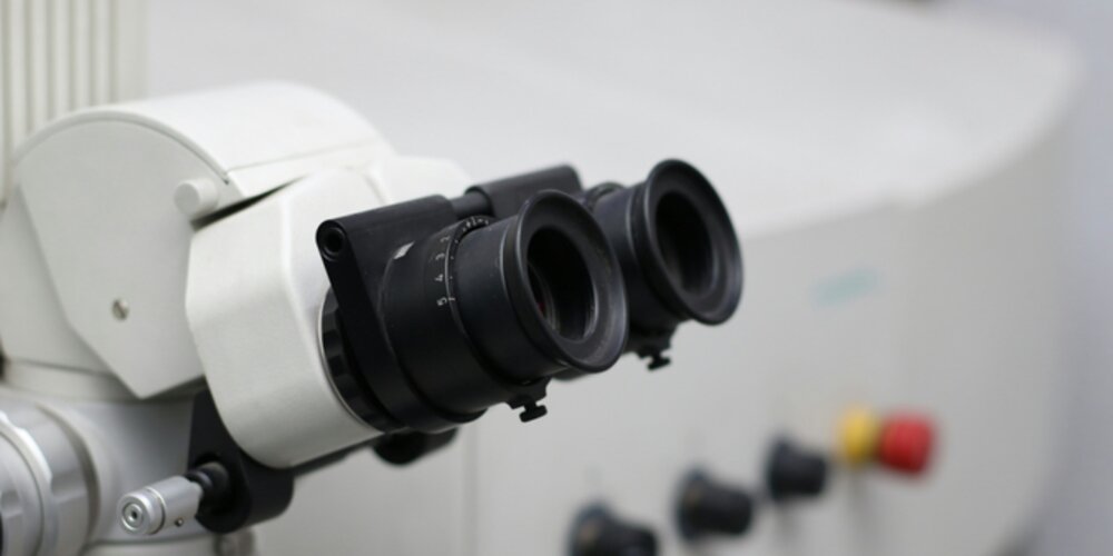
At The Lab, we’re at the cutting edge of materials testing technology to ensure our experts have everything they need to conduct valuable analyses and investigations.
Our digital microscopes are capable of a broad range of investigations, from weld analyses to microstructural inspections. Or, our scanning electron microscopy services can conduct a variety of tests, including inspecting non-conductive samples without the need for additional coatings.
Discover the uses of advanced digital microscopy at The Lab
For more of the latest news, industry advancements and insight, explore The Lab’s News and Knowledge Hub…
Researchers Create 3D Printed Components for Portable Mass Spectrometers | Researchers Find New Way to Weld Metal Foam Without Compromising the Material | ECTA Releases Their Annual Report 2023 & ECTA RC Report 2022
- Author
- Dr Holly Edwards
- Date
- 05/04/2024